- 您现在的位置:买卖IC网 > Sheet目录330 > IDT71T75802S200PFGI (IDT, Integrated Device Technology Inc)IC SRAM 18MBIT 200MHZ 100TQFP
IDT71T75602, IDT71T75802, 512K x 36, 1M x 18, 2.5V Synchronous ZBT? SRAMs with
2.5V I/O, Burst Counter, and Pipelined Outputs Commercial and Industrial Temperature Ranges
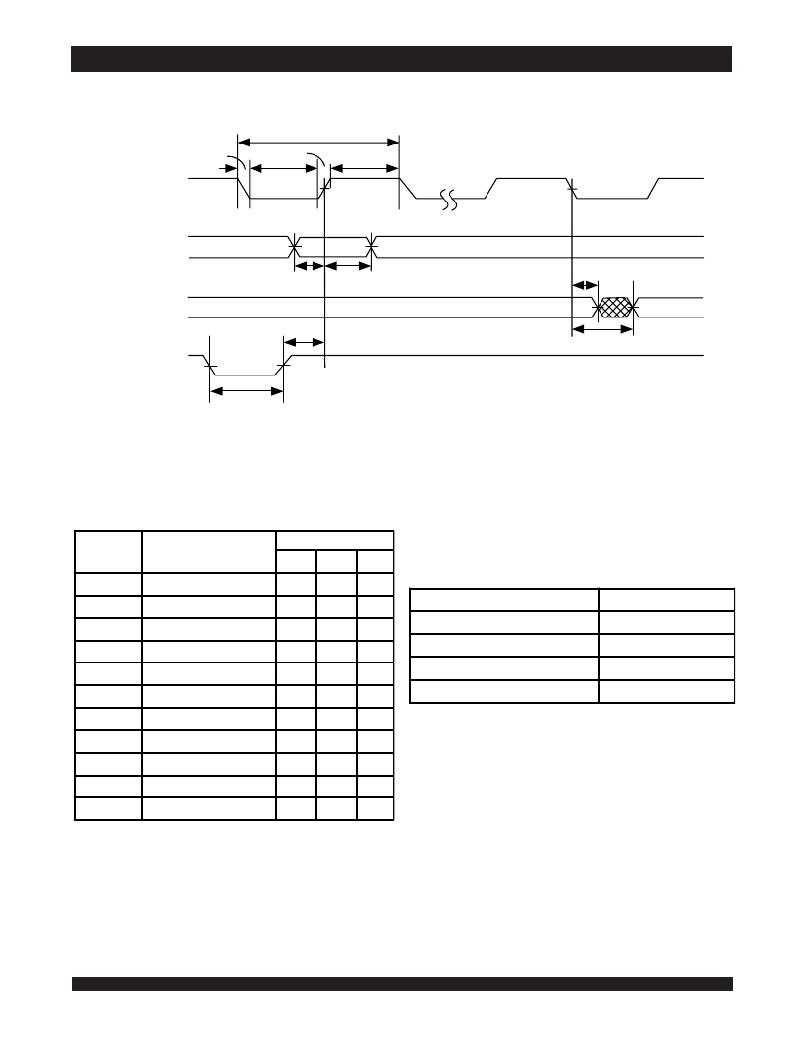
JTAG Interface Specification
t JCYC
t JF
t JCL
t JR
t JCH
TCK
Device Inputs (1) /
TDI/TMS
Device Outputs (2) /
t JS
t JH
t JDC
TDO
TRST ( 3)
t JRSR
t JCD
x
M5313 drw 01
t JRST
NOTES:
1. Device inputs = All device inputs except TDI, TMS and TRST .
2. Device outputs = All device outputs except TDO.
3. During power up, TRST could be driven low or not be used since the JTAG circuit resets automatically. TRST is an optional JTAG reset.
JTAG AC Electrical
Characteristics (1,2,3,4)
Symbol
t JCYC
Parameter
JTAG Clock Input Period
Min.
100
Max.
____
Units
ns
Scan Register Sizes
t JCH
t JCL
t JR
t JF
t JRST
t JRSR
JTAG Clock HIGH
JTAG Clock Low
JTAG Clock Rise Time
JTAG Clock Fall Time
JTAG Reset
JTAG Reset Recovery
40
40
____
____
50
50
____
____
5 (1)
5 (1)
____
____
ns
ns
ns
ns
ns
ns
Register Name
Instruction (IR)
Bypass (BYR)
JTAG Identification (JIDR)
Boundary Scan (BSR)
NOTE:
Bit Size
4
1
32
Note (1)
I5313 tbl 03
t JCD
t JDC
t JS
t JH
JTAG Data Output
JTAG Data Output Hold
JTAG Setup
JTAG Hold
____
0
25
25
20
____
____
____
ns
ns
ns
ns
1. The Boundary Scan Descriptive Language (BSDL) file for this device is available
by contacting your local IDT sales representative.
I5313 tbl 01
NOTES:
1. Guaranteed by design.
2. AC Test Load (Fig. 1) on external output signals.
3. Refer to AC Test Conditions stated earlier in this document.
4. JTAG operations occur at one speed (10MHz). The base device may run at any speed specified in this datasheet.
20
6.42
发布紧急采购,3分钟左右您将得到回复。
相关PDF资料
IDT71T75902S85BGG
IC SRAM 18MBIT 85NS 119BGA
IDT71V016SA12PHGI
IC SRAM 1MBIT 12NS 44TSOP
IDT71V124SA10PHGI
IC SRAM 1MBIT 10NS 32TSOP
IDT71V256SA20PZG
IC SRAM 256KBIT 20NS 28TSOP
IDT71V25761S200PFGI
IC SRAM 4MBIT 200MHZ 100TQFP
IDT71V30L35TFI
IC SRAM 8KBIT 35NS 64STQFP
IDT71V321L25TFI
IC SRAM 16KBIT 25NS 64STQFP
IDT71V3556SA166BGGI
IC SRAM 4MBIT 166MHZ 119BGA
相关代理商/技术参数
IDT71T75802S200PFGI8
功能描述:IC SRAM 18MBIT 200MHZ 100TQFP RoHS:是 类别:集成电路 (IC) >> 存储器 系列:- 标准包装:45 系列:- 格式 - 存储器:RAM 存储器类型:SRAM - 双端口,异步 存储容量:128K(8K x 16) 速度:15ns 接口:并联 电源电压:3 V ~ 3.6 V 工作温度:0°C ~ 70°C 封装/外壳:100-LQFP 供应商设备封装:100-TQFP(14x14) 包装:托盘 其它名称:70V25S15PF
IDT71T75802S200PFI
功能描述:IC SRAM 18MBIT 200MHZ 100TQFP RoHS:否 类别:集成电路 (IC) >> 存储器 系列:- 产品变化通告:Product Discontinuation 05/Nov/2008 标准包装:84 系列:- 格式 - 存储器:RAM 存储器类型:SRAM - 同步 ZBT 存储容量:4.5M(128K x 36) 速度:75ns 接口:并联 电源电压:3.135 V ~ 3.465 V 工作温度:-40°C ~ 85°C 封装/外壳:119-BGA 供应商设备封装:119-PBGA(14x22) 包装:托盘 其它名称:71V3557SA75BGI
IDT71T75802S200PFI8
功能描述:IC SRAM 18MBIT 200MHZ 100TQFP RoHS:否 类别:集成电路 (IC) >> 存储器 系列:- 产品变化通告:Product Discontinuation 05/Nov/2008 标准包装:84 系列:- 格式 - 存储器:RAM 存储器类型:SRAM - 同步 ZBT 存储容量:4.5M(128K x 36) 速度:75ns 接口:并联 电源电压:3.135 V ~ 3.465 V 工作温度:-40°C ~ 85°C 封装/外壳:119-BGA 供应商设备封装:119-PBGA(14x22) 包装:托盘 其它名称:71V3557SA75BGI
IDT71T75902S75BG
功能描述:IC SRAM 18MBIT 75NS 119BGA RoHS:否 类别:集成电路 (IC) >> 存储器 系列:- 标准包装:1,000 系列:- 格式 - 存储器:RAM 存储器类型:SRAM - 双端口,同步 存储容量:1.125M(32K x 36) 速度:5ns 接口:并联 电源电压:3.15 V ~ 3.45 V 工作温度:-40°C ~ 85°C 封装/外壳:256-LBGA 供应商设备封装:256-CABGA(17x17) 包装:带卷 (TR) 其它名称:70V3579S5BCI8
IDT71T75902S75BG8
功能描述:IC SRAM 18MBIT 75NS 119BGA RoHS:否 类别:集成电路 (IC) >> 存储器 系列:- 标准包装:45 系列:- 格式 - 存储器:RAM 存储器类型:SRAM - 双端口,异步 存储容量:128K(8K x 16) 速度:15ns 接口:并联 电源电压:3 V ~ 3.6 V 工作温度:0°C ~ 70°C 封装/外壳:100-LQFP 供应商设备封装:100-TQFP(14x14) 包装:托盘 其它名称:70V25S15PF
IDT71T75902S75BGG
功能描述:IC SRAM 18MBIT 75NS 119BGA RoHS:是 类别:集成电路 (IC) >> 存储器 系列:- 标准包装:1,000 系列:- 格式 - 存储器:RAM 存储器类型:SRAM - 双端口,同步 存储容量:1.125M(32K x 36) 速度:5ns 接口:并联 电源电压:3.15 V ~ 3.45 V 工作温度:-40°C ~ 85°C 封装/外壳:256-LBGA 供应商设备封装:256-CABGA(17x17) 包装:带卷 (TR) 其它名称:70V3579S5BCI8
IDT71T75902S75BGG8
功能描述:IC SRAM 18MBIT 75NS 119BGA RoHS:是 类别:集成电路 (IC) >> 存储器 系列:- 标准包装:45 系列:- 格式 - 存储器:RAM 存储器类型:SRAM - 双端口,异步 存储容量:128K(8K x 16) 速度:15ns 接口:并联 电源电压:3 V ~ 3.6 V 工作温度:0°C ~ 70°C 封装/外壳:100-LQFP 供应商设备封装:100-TQFP(14x14) 包装:托盘 其它名称:70V25S15PF
IDT71T75902S75BGGI
功能描述:IC SRAM 18MBIT 75NS 119BGA RoHS:是 类别:集成电路 (IC) >> 存储器 系列:- 产品变化通告:Product Discontinuation 05/Nov/2008 标准包装:84 系列:- 格式 - 存储器:RAM 存储器类型:SRAM - 同步 ZBT 存储容量:4.5M(128K x 36) 速度:75ns 接口:并联 电源电压:3.135 V ~ 3.465 V 工作温度:-40°C ~ 85°C 封装/外壳:119-BGA 供应商设备封装:119-PBGA(14x22) 包装:托盘 其它名称:71V3557SA75BGI
